


COB vs SMD vs GOB Fine pitch LED Display Technologies: Comprehensive Comparison of Advantages and Disadvantages
Click:
Comparison of COB, SMD, and GOB LED display technologies — covering structure, reliability, brightness, contrast, maintenance, cost, and real-world application suitability.
Structural Differences Among COB, SMD, and GOB LED Technologies
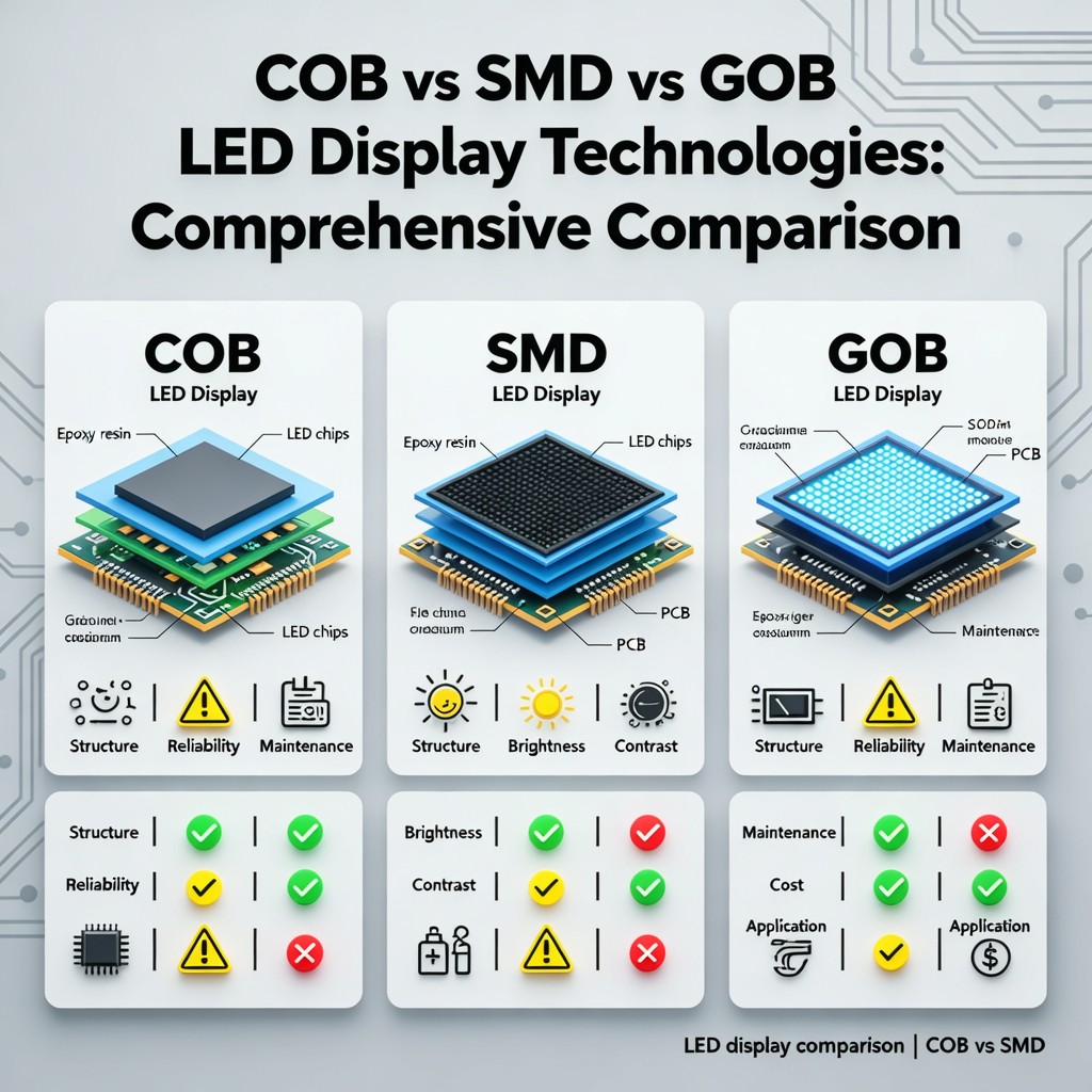
COB (Chip-on-Board), SMD (Surface-Mounted Device), and GOB (Glue-on-Board) represent three distinct approaches to LED packaging and pixel integration. SMD is the most mature and widely adopted method: individual red, green, and blue LED chips are encapsulated into discrete 3-in-1 or 4-in-1 surface-mount packages (e.g., 1010, 0808, 0606), then mounted onto PCBs using reflow soldering. COB integrates bare LED die directly onto a substrate—typically aluminum or ceramic—using wire bonding and global phosphor coating, eliminating individual lamp housings and solder joints. GOB, by contrast, is not a chip-level packaging technology but a protective enhancement applied *over* conventional SMD modules: a transparent, thermally conductive epoxy resin is dispensed uniformly across the entire display surface, sealing LEDs, solder joints, and circuit traces.
Reliability and Environmental Resilience
Reliability hinges on protection against moisture, dust, vibration, and thermal cycling. SMD displays—despite decades of refinement—remain vulnerable at solder joint interfaces and between individual LED packages, where micro-cracks and delamination can initiate under mechanical stress or humidity ingress. COB excels in intrinsic robustness: with no discrete packages or exposed solder points, it achieves superior resistance to impact, oxidation, and condensation. GOB significantly improves upon standard SMD reliability by forming a continuous, conformal barrier that prevents particle intrusion and dampens thermal expansion mismatch—making it ideal for semi-outdoor or high-humidity indoor venues like swimming pools, museums, or transportation hubs. However, GOB’s resin layer may yellow over time under intense UV exposure if not formulated with UV stabilizers, potentially affecting long-term color fidelity.
Brightness, Contrast, and Viewing Experience
Peak brightness (nits) is largely determined by LED chip efficiency and thermal management—not packaging alone—but packaging influences usable brightness and perceived contrast. SMD offers high luminance but suffers from visible black matrix gaps between pixels and reflective solder joints, reducing effective contrast ratio—especially in ambient light. COB eliminates inter-pixel gaps entirely due to direct die placement and integrated lensing, delivering seamless blacks, wider viewing angles (>170°), and higher effective contrast (often >10,000:1). GOB enhances SMD’s optical performance by suppressing reflection from solder joints and metal traces, improving black level uniformity and mitigating glare, though it cannot eliminate physical pixel pitch limitations inherent to the underlying SMD module.
Maintenance, Repairability, and Service Lifespan
SMD modules support component-level repair: defective LEDs or drivers can be desoldered and replaced individually, enabling cost-effective field maintenance. COB modules, however, are monolithic—failure of even one die typically necessitates full module replacement, increasing long-term service cost despite lower initial failure rates. GOB sits between these extremes: while the resin layer prevents direct access to solder joints and complicates rework, many manufacturers design GOB modules with standardized SMD footprints and accessible driver boards, allowing qualified technicians to replace entire modules without damaging adjacent units. All three technologies offer comparable rated lifespans (≥100,000 hours at L50), but real-world longevity depends heavily on thermal design and operating environment—not just packaging method.
Cost Considerations Across the Value Chain
Initial acquisition cost follows a clear hierarchy: SMD < GOB < COB. Standard SMD displays benefit from economies of scale, mature supply chains, and low assembly complexity. GOB adds ~15–25% premium over equivalent SMD modules due to precision dispensing equipment, material costs, and additional curing process steps. COB commands the highest upfront investment—often 30–50% above SMD—driven by specialized substrate materials, wire-bonding automation, stringent cleanroom requirements, and lower production yields. However, total cost of ownership (TCO) must account for reduced downtime, lower failure-related maintenance, and extended calibration intervals—areas where COB and GOB demonstrate compelling ROI in mission-critical or hard-to-access installations (e.g., ceiling-mounted retail signage or stadium perimeters).
Application Suitability and Real-World Deployment Guidance
Choosing among COB vs SMD vs GOB LED requires alignment with functional, environmental, and economic constraints. SMD remains optimal for budget-sensitive, high-volume applications with moderate environmental demands—such as corporate lobbies, educational facilities, and mid-tier digital billboards. GOB delivers the strongest value proposition where enhanced durability and visual quality are required without the full COB investment—ideal for shopping malls, airports, hospitals, and rental staging. COB is best reserved for premium, permanent installations demanding pixel-level uniformity, ultra-narrow bezels, and zero-maintenance operation—exemplified by broadcast studios, command centers, luxury retail environments, and fine-art digital canvases. Notably, pixel pitch continues to drive applicability: sub-P1.0 applications increasingly favor COB or advanced GOB-SMD hybrids, whereas P2.5 and coarser pitches remain dominated by high-reliability SMD variants.
In summary, COB LED, SMD LED, and GOB LED are not mutually exclusive alternatives but complementary solutions within the modern LED display ecosystem. Understanding their structural foundations, failure modes, optical trade-offs, and lifecycle economics enables integrators and end users to make evidence-based decisions aligned with technical requirements and strategic objectives.
In addtional, TEC Displays focus on COB technology from 2023 and develop on MOG technology for fine pitch LED video wall, follow us for more new technology in the near future.

点击右上角
分享给朋友吧


 Long by picture save/share
0
Add: Block 14, Tianliao No.5 Industrial Zone, Yutang Street, Guangming Dist, Shenzhen, Guangdong, China 518132
Follow TEC
Follow TEC